Menu
-
 Motors
-
 Electronic Components
Electronic Components
Electronic Components-
 Microcontrollers
-
 Integrated Circuits
-
 Transistor
-
 Thyristor / Triac
-
 Mosfet
-
 LED
LED
-
 Resistor
-
 Potentiometer
-
 Trimpot
-
 Diode
Diode
-
 Capacitor
-
Connectors
Connectors
- Waterproof Connector
- Military Type Connector
- Mike Connector
- Terminal Block
- Power Connector
- Header
- SMA Connector
- Pogo Pin
- Banana Jack
- Born Jack
- Battery Clip
- Canon Jack
- D-Sub Konnektör
- Dip Switch
- JST Connector
- Tamiya Connector
- Stereo - Mono Jack
- BNC Connector
- Test Clips
- DIN Connector
- Auto Cigarette Lighter Socket
- FFC/FPC Connector
- Other Connectors
- See All
-
 Crystal Oscillator
-
 Fuse and Slots
-
 Joysticks
-
 Thermal Fuse
-
 USB Chassis
-
 Reed Relay
-
 Transformer & Voltage Converters
-
 Peltier
-
 Pastes
-
 Optocoupler
-
 Coil
Coil
-
 Other Components
-
 NTC/PTC
-
 Relay
Relay
-
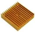 Coolers and Insulators
-
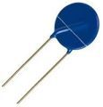 Varistor
- See All
-
-
 Arduino
-
 Raspberry Pi
-
 Robot Kits
-
 Educational Kits
Educational Kits
Educational Kits -
 Sensors
Sensors
Sensors -
 3D Printer and Filament
3D Printer and Filament
3D Printer and Filament -
 Drone and Multicopter
-
 Motor Driver Cards
Motor Driver Cards
Motor Driver Cards -
 Voltage Regulator Boards
Voltage Regulator Boards
Voltage Regulator Boards -
 Relay Cards
-
 Buttons and Switches
Buttons and Switches
Buttons and Switches- Metal Button
-
Rocker Switch
Rocker Switch
-
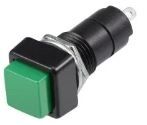 Push Button Switch
-
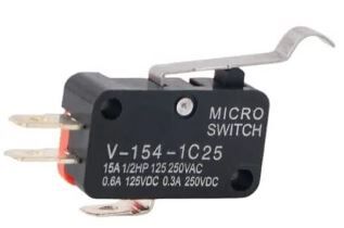 Micro Switch
-
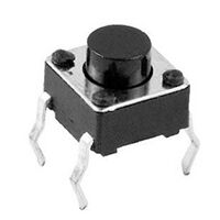 6X6 Tact Switch
-
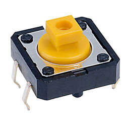 12X12 Tact Switch
-
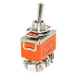 Toogle Switch
-
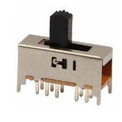 Slide Switch
-
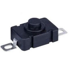 Tact Switch
-
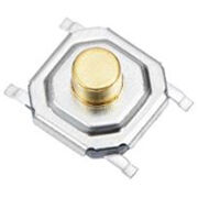 SMD Tact Switch
-
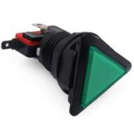 Game Machine Buttons
-
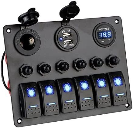 Marine Switches and Panels
-
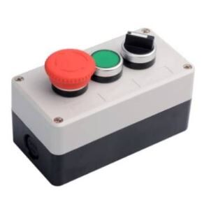 Button Box
-
 Membrane Button
-
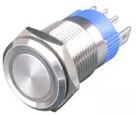 Metal Push Button
-
 Special Buttons
-
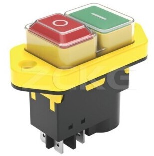 Elektromanyetik Switch
- See All
-
 Automation Equipments
-
 Screens
-
 Electronic Boards
-
 Li-po Batteries
Li-po Batteries
Li-po Batteries-
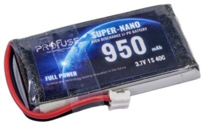 1S 3.7V Lipo Battery
-
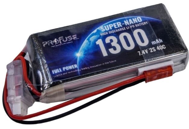 2S 7.4V Lipo Battery
-
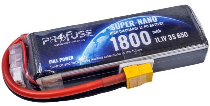 3S 11.1V Lipo Battery
-
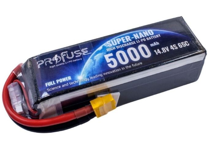 4S 14.8V Lipo Battery
-
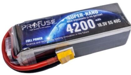 5S 18.5V Lipo Battery
-
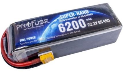 6S 22.2V Lipo Battery
-
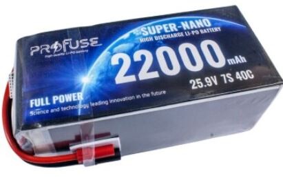 7S 25.9V Lipo Pil
-
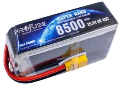 8S 29.6V Lipo Pil
-
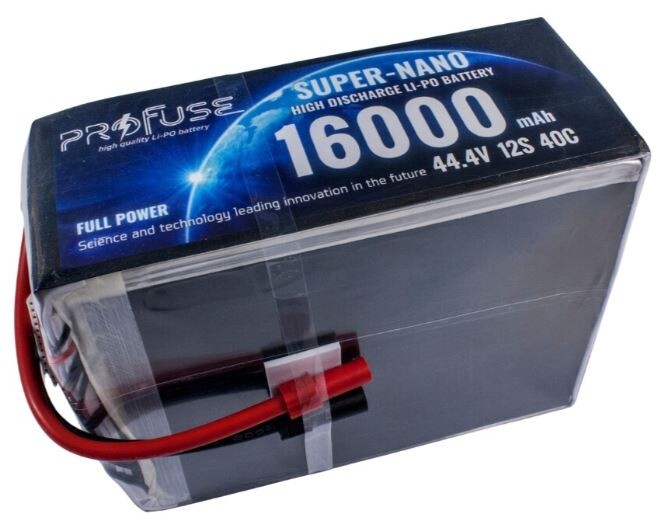 12S 44.4V Lipo Battery
-
 Solid State Lipo Pil
-
 Airsoft Lipo Battery
-
 Drone Batteries
-
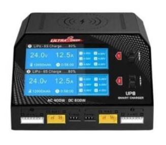 Lipo Chargers
-
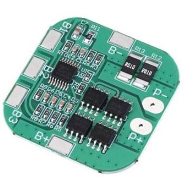 Lipo Charging and Balancing Boards
-
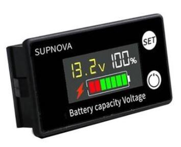 Lipo Indicators
-
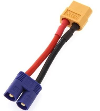 Lipo Battery Cables
-
 Lipo Battery Safe Bags
-
 Lipo Battery Belts
- See All
-
-
 Battery - Lead-Acid Battery - Solar Panels
Battery - Lead-Acid Battery - Solar Panels
Battery - Lead-Acid Battery - Solar Panels -
 Power Supplies
Power Supplies
Power Supplies -
 Wireless Communication
Wireless Communication
Wireless Communication-
 Bluetooth
-
 WIFI
WIFI
-
 RF Module
-
 GPS/GPRS/GSM
-
Antennas and SMA Connectors
Antennas and SMA Connectors
- See All
-
-
 Measurement and Testing Instruments
-
 Soldering Iron and Equipment
Soldering Iron and Equipment
Soldering Iron and Equipment -
 Cables and Converters
-
 Copper Plaque and Breadboard
Copper Plaque and Breadboard
Copper Plaque and Breadboard -
 Hand Tools and Hardware
Hand Tools and Hardware
Hand Tools and Hardware-
 Screwdriver
-
 Side Chisel - Pliers
-
Magnet
Magnet
-
 Heat Shrink Tubing
-
 Tweezers
-
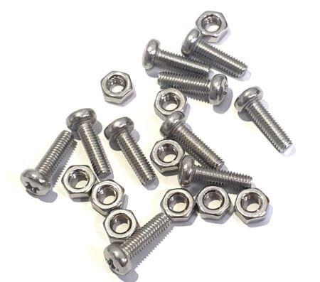 Screw/Nut
-
 Drills and Drill Bits
-
 Silicone Gun
-
 Sprays
-
 Cable Tie
-
 Organizer Boxes
-
 Antistatic ESD Wristband
-
 Chuck
Chuck
-
 Tape Types
-
 Crimping and Stripping Pliers
-
Electronic Nail Drill Set
Electronic Nail Drill Set
-
 Other Hand Tools
- See All
-
-
 Speaker and Buzzer
Speaker and Buzzer
Speaker and Buzzer -
 Wheels
-
 Mechanical Parts
- Outlet
- Contact Us
Close
Cart
.png)
 Geared DC Motors
 DC Motors Without Gearbox
 Stepper Motors
 Servo Motors
 AC Motors
 Linear Motors
 Solenoid Coil - Valve
 Electromagnetic Valve
 Vibration Motors
 DC Motors with Encoder
 Air and Liquid Pumps
 Fans
Fans
 Spindle Motors
 Special Motors
 Actuators
 Gear Boxes
 Microcontrollers
 Integrated Circuits
 Transistor
 Thyristor / Triac
 Mosfet
 LED
LED
 Resistor
 Potentiometer
 Trimpot
 Diode
Diode
 Capacitor
 Crystal Oscillator
 Fuse and Slots
 Joysticks
 Thermal Fuse
 USB Chassis
 Reed Relay
 Transformer & Voltage Converters
 Peltier
 Pastes
 Optocoupler
 Coil
Coil
 Other Components
 NTC/PTC
 Relay
Relay
 Coolers and Insulators
 Varistor
 Original Arduino Models
 Clone Arduino Models
 Arduino Shield
 Arduino Sets
 Arduino Modules
 Arduino Boxes
 Raspberry Pi Models
 Raspberry Pi Electronic Boards
 Raspberry Pi Screens - LCD Display
 Raspberry Pi Camera
 Raspberry Pi Enclosures
 Raspberry Pi Accessories
 Raspberry Pi Cables
 Wheeled Robot Kits
 Tracked Robot Kits
 Humanoid Robot
 Gripper
 DIY Robot Kits
 Makeblock
 Robobloq
 Evo Stem Kits
 DIY Training Kits
 DIY Electronics Kits
 Bellrobot
 Object / Line / Distance
 Temperature, Humidity Sensors
 Accelerometer
 Light, Color
 Pressure / Compass
 Current / Voltage
 Signal Generator Modules
 Gas Sensors
 Weight Sensors
 Touch Sensors
 Biometric / Medical
 Force / Vibration
 Sound Sensors
 Laser
Laser
 Magnetic / Encoder
 Mercury Sensors
 Other Sensors
 3D Printer
 3D Pen
 Filament
 3D Printer Electronic Parts
 3D Printer Mechanical Parts
 3D Printer Other Parts
 CNC
CNC
 Drone Motors
 Flight Control Boards
 Drone Controller 2.4 Ghz
 Brushless Motor Drivers - ESC
 Drone Bodies
 Drone Kits
 Drone Propellers
 Other Drone Parts
 Ac Motor Drivers
 Dc Motor Drivers
 Servo Drivers
 Stepper Motor Drivers
 Step-Down Boards
 Step-Up Boards
 AC-DC Converter
 Optokuplör
 Other Voltage Regulators
 5V Sequential Relay Cards
 12V Sequential Relay Boards
 Timed Relay Boards
 Temperature and Humidity Adjustable Relay Boards
 USB Relay Boards
 Solid State Relay Boards
 IR Controlled Relay Boards
 Other Relay Boards
 Push Button Switch
 Micro Switch
 6X6 Tact Switch
 12X12 Tact Switch
 Toogle Switch
 Slide Switch
 Tact Switch
 SMD Tact Switch
 Game Machine Buttons
 Marine Switches and Panels
 Button Box
 Membrane Button
 Metal Push Button
 Special Buttons
 Elektromanyetik Switch
 Buttons and Signal Lamps
 Switches
 Industrial Fans and Filters
 Cable Ferrules
 Rail Type Power Supplies
 Thermocouple
 SKP/FITTING
 Busbar Insulator
 Digital Display
 Touch Screens
 Dot Matrix Display
 Graphic LCD Screens
 Character LCD Display
 Keypad
 Oled LCD Display
 Segment Display
 TFT Screens
 Development Boards
 Microcontroller Programmers
 Amplifier Boards
 Induction Heating Boards
 Modules
 NeoPixel
 Converter Boards
 SMD DIP Converter
 1S 3.7V Lipo Battery
 2S 7.4V Lipo Battery
 3S 11.1V Lipo Battery
 4S 14.8V Lipo Battery
 5S 18.5V Lipo Battery
 6S 22.2V Lipo Battery
 7S 25.9V Lipo Pil
 8S 29.6V Lipo Pil
 12S 44.4V Lipo Battery
 Solid State Lipo Pil
 Airsoft Lipo Battery
 Drone Batteries
 Lipo Chargers
 Lipo Charging and Balancing Boards
 Lipo Indicators
 Lipo Battery Cables
 Lipo Battery Safe Bags
 Lipo Battery Belts
 18650 Battery and Accessories
 Battery
 Battery Slots
 Solar Panel
 Lead-Acid Battery
 Powerbank
 Charging Modules
 Adapters
 Power Supplies
 Regulated Power Supplies
 Bluetooth
 WIFI
WIFI
 RF Module
 GPS/GPRS/GSM
 DC Voltaj, Akım ve Watt Ölçer
 AC Voltaj, Akım ve Watt Ölçer
 Digital Multimeter
 Clamp Meter
 LCR Meter
 Oscilloscope
 IR Thermometer
 Meger Devices
 Electrical Installation Testing Devices
 Analog Multimeter
 Other Measuring Instruments
 Probes
 Soldering Iron
 Soldering Iron Stations
 Solder Wires
 Solder & Soldering Iron Pumps
 Soldering Iron Stand
 Flux
Flux
 Solder Pastes
 Soldering Iron Tips
 Jumper Cables
 Installation Cables
 JST Cable
 Converter & Jack
 Computer Cables
 Adjacent and Shielded Cable
 Flat Cable
 Crocodile Cable
 Braided Ground Cable
 Silicone & Glass Fiber Cables
 Breadboard
 Copper Plaque
 Conductive Materials
 Pnp Paper
 Screwdriver
 Side Chisel - Pliers
 Heat Shrink Tubing
 Tweezers
 Screw/Nut
 Drills and Drill Bits
 Silicone Gun
 Sprays
 Cable Tie
 Organizer Boxes
 Antistatic ESD Wristband
 Chuck
Chuck
 Tape Types
 Crimping and Stripping Pliers
 Other Hand Tools
 Buzzer
 Microphone
 Snap-On Wheels
 Terrain Wheels
 Caster Wheels
 Omni Wheels
 Silicone Wheels
 Motor Holders
 Sensor Holders
 Robot Bodies
 Coupling
 Servo HUB
 Spacer / Distance
 Plastic Gears
 Propellers


